
For a certain number of projects, including first-prototype, surface mount 'breadboarding', layout experimentation, rapid multiple-revisions, and 1-hour deadlines doing your own PCB etching can be quick, clean, and very very inexpensive. The method set up in the Media Lab basement is somewhat-similar to that of large pcb manufacture shops, except in scale and automation. There is no system for through-hole plating, automated drilling/routing or multilayer design. However, you can make precisely aligned doublesided boards with simple registration techniques.
Added 2/7/04: The etching setup is now in the Holography darkroom, in the LL across from the shops. To get access/training please email or visit me (ladyada@ml in office 020D)
Added 2/7/05: Ha! I graduated. Bug someone else in the Computing Culture group...
A tool is only good towards the application it was designed for. Using the etcher for something other than what its good for will frustrate you and waste time.
When using the spray etcher is a good idea:
- You need the boards quickly
- The substrate is 1/16" with 1oz or 2oz copper either FR4 or paper phenolic (preferred)
- The design is single sided
- There are many surface mount parts
- The design is double sided, with no hidden vias (vias underneath surfacemount parts) or through-hole part vias (vias that also serve as through-hole component holes) that you cannot solder on both sides
- You can visually scan for shorts
- The design follows a 12/12 mil rule (this is probably not true, I'm sure 10/10 or even 8/8 is fine, but yield will drop) That is, 12mil minimum trace width, and 12mil minimum trace distance.
- You only need a few boards, or are willing to live with a yield as low as 50%
- Drill hole locations can be imprecise (up to 10 mils off!)
Conversely, when using the spray etcher is a bad idea:
- You dislike wet chemistry/cleaning
- Are using exotic substrates
- There are many vias, or throughhole parts, and you dont want to drill holes/solder vias.
- You want the boards to be perfect without checking for shorts or opens
- You need printed overlays, multiple layers, through hole plating or solder masks.
- You want many parts. Remember that for $200 you can just about get as many boards as your heart desires, and from a reputable PCB manufacturer.
In this step you will prepare your layout for etching. For this step you will need: a quality laser printer, a sheet of transluscent paper.
The photoresist method we use in PCB etching is a positive process, which means that when UV light hits the resist, it softens, and then is washed away. What remains is a positive of the PCB design. What this boils down to is that you will want a positive printout of your PCB design (black where there will be copper). Preferably mirrored. Most all PCB design tools let you print out your layout mirrored. Or you can mirror your entire design in the software. Whichever. Also, if possible, have it print white holes where you will drill, these will be your drill guides. Because the drill holes will not be precise, make your annular rings (the copper around a drill hole) larger than normal. Since you will lose as many as half of the design to exposure/development/etching flaws, tile 2-3 times layouts as many as you want.
In Eagle: After your design is ready, go to the CAM Processor, and open the "layout2.cam" job. As output select PS. Change the extention to ".ps" as well. Be sure that Mirror is selected but that Fill Pads is not. Then open the ps with any free postscript viewer and print it. (Also you could print it to "Gerber274x" and use a gerber viewer, or any other format you can print.)
After you have verified the above, print your design to a high quality (600dpi at least) laser printer, in monochrome mode, onto a white piece of paper. Double check that it is as you want it, in the correct orientation, enough tiling, mirrored, dark ink, slightly smaller than the PCB you have, etc. Now print it onto translucent paper, there is a box of it in the cabinet underneath the etcher, in a thin cardboard sleeve.

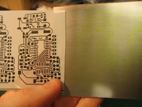
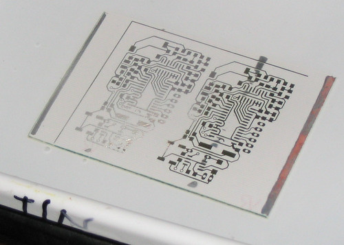
Left, plain paper test. Right, translucent paper. Both are mirrored.
In this picture, I have two layouts I want to etch. I tiled one three times and one twice. The one I tiled three times has a very fine pitch IC (TSSOP-16) so it is less likely to come out. On the left is opaque laser print. On the right, translucent paper. Note that the design (noticably the text) is mirrored.
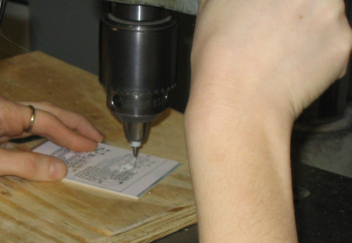
This step transfers your layout design to a positive-resist PCB by exposing UV light to the sensitized PCB with the printout as a mask. For this step you will need: a presensitized positive photoresist copper clad board, scissors, tape, a UV bulb and thin plate glass or exposure unit. This step takes 5-10 minutes.
First cut out the layout leaving a few millimeters of space on the edges. If you are going to perform the exposing and etching in the same session, go ahead and turn the etching machine on now, since it takes 10 minutes to warm up.
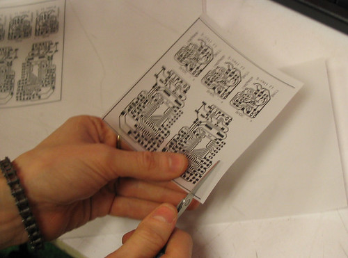
Cut the translucent paper, leaving at least a few mm boarder
Next, locate an unused PCB. There is a bag of them in the cabinet underneath the etcher. You may need to cut a larger board down using a metal shear. Using a larger PCB than necessary is wasteful, and exhausts the chemicals faster than a board that is well-fit. You can also purchase your own stash of PCB material in many different substrates, thicknesses, etc. and, of course, that is encouraged. (See "Where to Purchase Supplies, at bottom")
The best PCBs are those that have a plastic sticky sheet protecting them (some are just sold in a plastic bag) so that they can be handled, drilled and sheared without excess UV exposure. The plastic is easy to peel off:
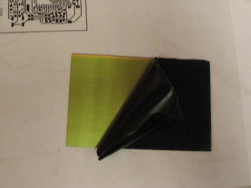
The underlying substrate should be a greenish colour
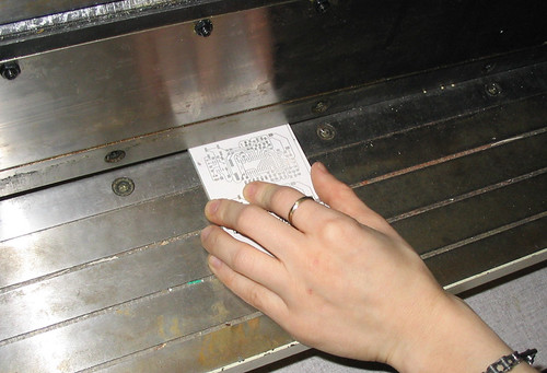
Place your design on top of the exposed resist, ink-side down, so that it appears not-mirrored when you look through the paper at the board. Placing the ink closest to the resist means less light can leak around and cut into thin traces. Next, tape down the design on two edges, so that the tape does not overlap any of the layout, but holds the paper flat.
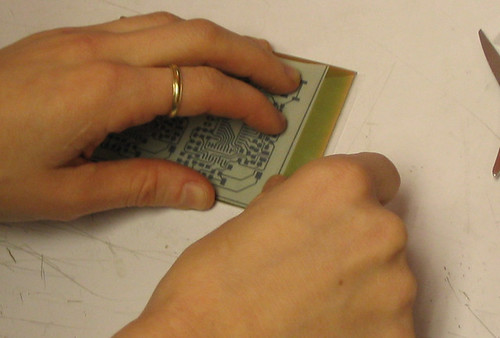
Use any plain tape to tape down two opposite sides without overlapping the layout
now take it to be exposed under a UV lamp. As an arbitrary measure, a 15W Sylvania "350 Blacklight" UV 24" flourescent bulb, 3" above a FOTOBOARD2-brand board, with a 1/8" clear glass plate (to keep the paper totally flat) over the board, 10 minutes will give good exposure. [When a more permanent fixture is found, it will be calibrated.]
After it has been exposed, peel off one piece of tape and flip it open, to look at the photoresist. Well exposed photoresist is a paler green, and you will be able to see the layout in the original, yellower green, faintly. If you don't see anything, retape that side, and try a few more minutes under the lamp.
The unexposed part is faintly visible, on the right side.
Once you think you're done exposing, lift off the design and put it away in case you want to make another set of boards. You are ready to perform the chemical processing. If you need to do this part later, or you have other boards to expose, place this board in an opaque container (like in an envelope, face down, in a drawer or somesuch.)
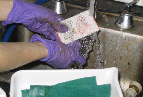
In this step, the exposed photoresist is removed chemically using developer, leaving a positive of your layout in photoresist on copper. For this step you will need: gloves, apron, sink, dev tray, developer, small soft sponge. This step takes 3 minutes.
Take the board over to your processing area. Put on the apron and a pair of 'rubber gloves'. These wet chemicals can splash, some stain, and they are not good to drink. Find the dev tray and the bottle of developer, (both marked DEV) and make sure the tray is clean. There is one set of large trays (for > 5x7") and one small set, use the ones that fits best. Place the board face up in the tray and pour developer in until there is about 1/4" (or enough to cover) in the tray.
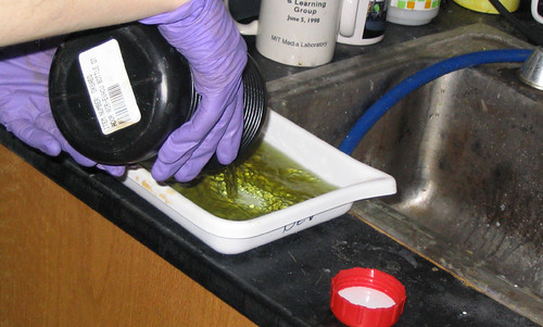
Carefully pour into a tray. The developer is green from use, it starts out clear
Almost immediately the board will start to 'leak' resist as it is attacked by developer. Agitate the board with your hand, and swirl the developer around to make sure there is a flow around the board. It should be developed in 1/2 to 1 minute. If you leave it in too long, some of the finer traces wont come out. Leaving it in too little means that there will be a very thin, invisible, layer of resist left that will stop the etching process and force you to repeat this step. Use a soft sponge to wipe the photoresist away.

Before rinsing, rub down the board with a soft cloth or sponge soaked in developer
Rinse the board in cold water to clean off the developer (stop bath), the parts that are to be etched should look like competely clean copper, no residue. If you feel a slimy/slippery coating, or see a bluish coating, you need to develop more. If none of the resist came off, you'll need to realign your paper and reexpose the board. Pour the developer back into the bottle, and rinse off the tray. The board is now ready to etch.
A well developed board has solid green traces and a clean copper background
In this step, the board is spray rinsed to prepare it for etching. This step takes 2 minutes.
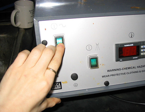
First check to see that the machine is on. If not, turn the machine on.
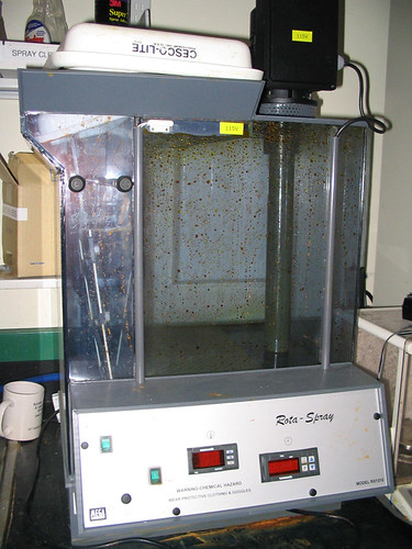
The Rota-Spray machine, the wash tank is on
the left, the etching tank on the right.
The on button is in the top left corner.
Once on, the left LED display should display "oC" and then something like "23" which means the etchant is at 23degC. Now load the board into the board holding apparatus, placing it near the center, and securing the plastic nuts. Make sure the board wont fall out and into the tank.
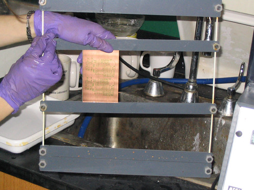
The board holder can hold many small boards, but make sure they cant fall out
Slide the board holder, with the copper facing right, into the wash tank. Attach the water hose (black, with white plastic spring-end) to the sink faucent, and turn on the cold water.

The connector is a little difficult to use, requiring that you simultaneously push down on the ring while pressing the brass fitting into the faucet head. Two handed might be easier at first.
Turn on the wash spray to clean off the board. You can move the holder up and down to make sure the board is sprayed off.
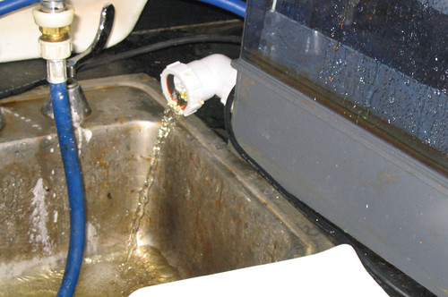
Make sure the water drains cleanly into the sink. This is the older setup, in the current lab there should be a PVC drainage pipe into the large sink so there shouldnt be any drain problems
In this step, the board is placed in an etcher, which is a machine that washes warm ferric chloride (or another etchant) over the board, eating away any exposed copper. For this step you will need to make sure the etchant is warm enough to use. This step takes 2minutes.
Move the holder into the etching tank, again facing to the right. Check that the temperature monitor reports 42-45 degrees C, and that the fluid well feels warm. also make sure the top is secured so that there is very little chance FeCl will spray out the top. By default the timer is set for 1:30 minutes, which I've found satisfactory. You can also change the time if necessary (for different weights of copper). Turn on the spray pump by pressing start. The entire tank will turn reddish brown as the etchant removes the copper from your board. After the time is up, remove the holder and quickly put it in the wash tank again. Be careful as there will be a lot of FeCl dripping off the holder and you dont want it going anywhere but in the machine or the sink.
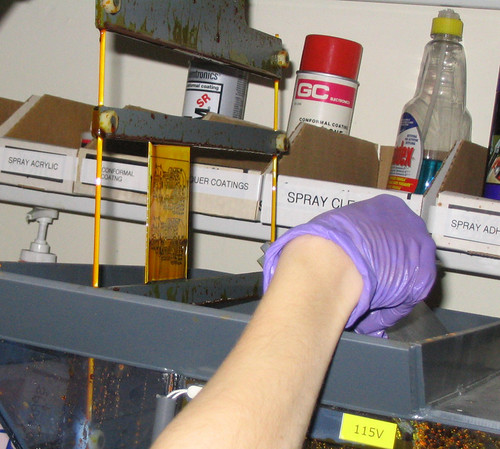
The board is very messy at this point, so do the move quickly and carefuly
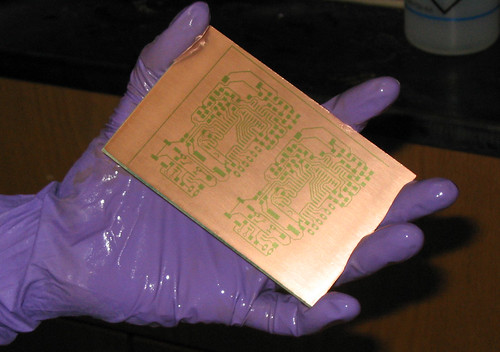
Turn on the wash spray again, moving the holder around so that the entire board and holder are completely cleaned off. After the water runs clean, remove the board and examine it. There may be parts that didn't etch, or overetched. Depending on your patience and yield, you may decide to re-etch a subset of your boards.
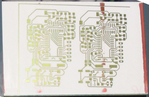
There are some traces of unetched copper on the right. Since I only needed one PCB, I just threw it away.
Examine all the boards carefully to determine which ones have shorts/opens/missing traces/etc, and which ones are good for use. Shut off the water faucet, run the spray to clean out the hose, turn off the machine and disconnect the hose from the faucet.
In this step, the remaining photoresist is stripped away, leaving only copper. For this step you will need chemical stripper and/or a scrub pad. This step takes 2 minutes.
Place the board face up in the STRIP tray, and coat it with resist stripper. This may be in a bottle or in a 'shoepolish' dispenser. Rub in the chemical first with the soft sponge, then with with a plastic scrub pad. The green resist should come off, revealing copper underneath. Make sure -all- of the resist is removed, as it smells very bad when it gets hot (when soldering.) If there is no stripper, you can just scrub it off with a green scrub pad. If the stripper came from a bottle, pour it back in. Rinse off the board and tray.
You can easily remove the resist with just a green scouring pad
This step is optional but is very helpful for soldering to your board. For this step you will need: tinning liquid mix. This step takes 2-10 minutes.
Find the bottle of tinning liquid, and the TIN tray. Place the board in the tray copper up, and pour in enough tinning liquid to cover the board, the copper should immediately turn a silvery color. If you intend to reflow solder, you may want to leave it for 15 minutes, otherwise, 3-5 is probably fine. Use this time to clean up the area around the etcher, rinse off surfaces and clean and dry any trays. When the board is done, remove and rinse it. Pour the tinning liquid back into the bottle and clean the tray. Throw away the gloves, and put the apron back. Make sure the area looks better than it did when you got there.
The exposed copper will turn silver almost immediately, tin will aid soldering and stop oxidation
In this step, any holes or vias in the PCB are drilled out. For this step you will need: a drill press that can run at 2000+ RPM, high-speed carbide wire-gauge drill bits. This step takes 3-10 minutes, depending on number of holes in pcb.
If your PCB is FR4 laminate, you may want to find a dust mask for this step, since fiberglass dust is carcinogenic. Chances are, you're using paper phenolic which is much safer. There is a box of HSS carbide drill bits in a box underneath the etcher, they are packaged in plastic boxes of 10. Find the boxes of closest size to your board holes. In general, .020"/75ga is good for RF vias, .028"/70ga is good for signal vias, .035"/65ga is good for DIP/LEDs/Resistors/Capacitors, etc., .042"/58ga is good for TO-220/heavier diodes/etc., .060"/53ga for heavier wires and power components, and .086"/44ga for mounting holes or anything else. Other drill sizes are available for purchase, of course.
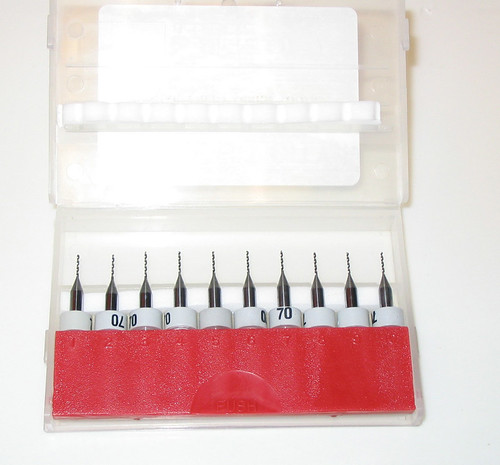
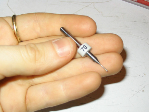
Left, these are inexpensive resharpened drill bits $7.50 a box. Right, 70 gauge is as small as you'll need
Place the first drill bit in the chuck, and tighten it well. Find a piece of wood to place underneath the board for support. While the drill is running, adjust the speed to 2000RPM or higher.

The drillpress in the media lab shop is more than sufficient, adjust it only while running
Drill all holes of one size at a time. Try to position the drill bit right in the center of the hole, or at least, try not to drill through any copper traces. The drill bits might break, especially if they sub-35mil. Holding the board steady while drilling through it helps. The bits only cost 75 cents so just throw them away when broken, but if you break more than 5, you should purchase a replacement set.
You can drill a hole a second if you dont clamp down the board, but breakage is more likely
After all the drilling, replace the bits in their boxes, and put the box back underneath the etcher.
In this step, the tiled layouts are seperated. For this step you will need a metal shear (this step could also be done with a band saw.) This step takes 2 minutes.
Shear or cut the good boards out, leaving a few mm on each edge. The edges may be filed or sanded.
A metal shear, such as the one outside the shop, is good for this. Go slowly and use the middle
Congratulations, you have finished your first home-made PCB!
- A single sided pcb is the simplest design possible, which you may outgrow...
- Making good registered double sided PCBs
- Using the Modela (or any other mini-mill) to do all the through-holes before etching
- Laminating dry-film photoresist onto copper-clad boards
- Plated through-hole vias (requires more chemistry and another machine)
There are two supply houses I use for general supplies:
- Vital Presentation Corp. (VPC Inc.) - a reseller for MegaUK. Sells virtually everything for etching. They dont have an online catalog, so look at MegaUK's site first.
- Think & Tinker - has a slightly different approach to PCB design, that allows for plated through holes, but requires that you laminate the photoresist yourself. They sell all sorts of chemicals and machines and supplies.
- Digikey - Of course, they sell everything and sometimes they even have some etching supplies...Not precisely sure whether they are compatible. Development/Exposure times may vary.